|
Silicon Solar Cells & Antireflection Coating |
|||||
Laser Annealing
Nanopaticle Stacks
(INC) method
Silicon Solar Cells & Antireflection Coating Nanoparticles Nanoimprint & Nanofabrication Organic Solar Cells Carbon Nanotube |
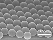
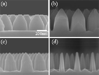
NanoSphere Lithography Nanosphere Lithography (NSL), or so-called Colloidal lithography (CL) is a low-cost and relatively high-throughput technique for patterning nanostructures. The advantage of colloidal lithography in nanofabrication is that large-area self-assembly of colloids having well-ordered structures can be performed without the need for expensive equipment. Recently, nanostructures such as rings, dots, and rods have been fabricated using colloidal lithography. Exploiting the index-matching concept, monolayer nanoparticles also have been used for the antireflective layer on glass substrates that lack optimally textured structures. As shows in Fig.1, we demonstrate a simple method—one that combines close-packed monolayer and bilayer nanospheres with an optimal one-step reactive ion etching process—for fabricating and optimizing the performance of pyramidal and honeycomb-like antireflection structures in subwavelength scales. We believe that colloidal lithography has great potential for use in the preparation of high-performance textured structures in large-area solar cells at low cost and with high reproducibility. Fig. 2 displays top-view and cross-sectional images of the different textured profiles obtained after varying the duration of etching for the one-step process. Fig. 2 (a) indicates that etched silicon having a height of ca. 310 nm and a small, flat roof appeared when the etching was performed for 35 s. Upon increasing the etching duration, the top of the etched silicon became sharper and the width narrower. Progressing from Fig. 2 (b) to (d), the height of etched silicon increased to 480 nm (60 s) then decreased to 380 nm (150 s). From the top-view images, we observe that the texture area decreased upon increasing the duration of etching. |
|
|||
Copyright(c) 2008 Nano-optpelectronics Lab., Department of Material Science and Engineering, National Taiwan University No. 1, Sec. 4, Roosevelt Road, Taipei, 10617 Taiwan(R.O.C) Phone:+886-2-3366-4076 Fax:+886-2-2362-7651 |
|||||