|
Nanoimprint & Nanofabrication |
|||||
Laser Annealing
Nanopaticle Stacks
(INC) method
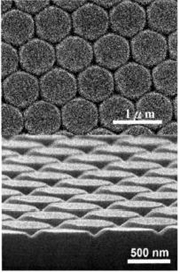
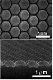
Silicon Solar Cells & Antireflection Coating Nanoparticles Nanoimprint & Nanofabrication Organic Solar Cells Carbon Nanotube |
Directly nanoimrpinting ferroelectric films We demonstrate an imprint method for patterning ferroelectric films. In contrast to conventional nanoimprint lithography, the patterned mold is directly imprinted in a ferroelectric film or a metal/ferroelectric film bilayer structure. In general, direct imprint in a ferroelectric or metal film needs ultrahigh pressure or temperature to form patterns. In this article, the authors improve the direct imprint processes by using a sharp mold and an underlying soft gel film for the reduction of the imprint pressure and temperature. The imprint pressure can be reduced to be compatible with the conventional nanoimprint instrument. The authors also successfully use the metal/ferroelectric bilayer structure to overcome the pattern flattened problem in a gel film. The cover metal layer can also be the upper conductive layer in the ferroelectric application. For direct contact of the metal film with mold, no surfactant should be coated on the surface of mold. It also indicates that no mold-rework processes are necessary for this direct imprint ferroelectric film method. |
|
|||
Copyright(c) 2008 Nano-optpelectronics Lab., Department of Material Science and Engineering, National Taiwan University No. 1, Sec. 4, Roosevelt Road, Taipei, 10617 Taiwan(R.O.C) Phone:+886-2-3366-4076 Fax:+886-2-2362-7651 |
|||||