|
Semiconductor processes and nanofabrication |
|||||
High-efficiency photo-electron conversion devices Semiconductor processes and nanofabrication Characterizations and applications of nanomaterials Optical characterization of graphene Graphene-gold oxide photodetector Optical analysis of hollow gold nanoparticles Photomodification of hollow gold nanoparticles for high-density data storage Light harvesting and light extraction Light extraction efficiency of LEDs Antireflection structures for solar cells Optical analysis techniques Eco-friendly devices and sensors
|
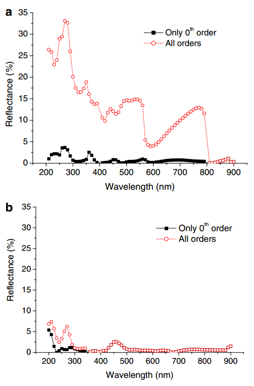
Fabrication of sub-wavelength antireflective structures in solar cells by utilizing modified illumination and defocus techniques in optical lithography We demonstrate a simple method, which is combining modified illumination and defocus techniques to fabricate sub-wavelength antireflective structures for solar cells. The optimum pyramid resist and silicon profiles can be obtained after exposure, development and common dry etching processes. The reflection and transmission properties are analyzed by the rigorous coupled-wave analysis in two-dimensional microstructure and find the reflectance is dramatically increased as consideration of all diffraction orders. Therefore, patterning the sub-wavelength texturing structures for eliminating the diffraction order light is important. Patterning sub-wavelength structures should use the short wavelength combining defocus exposure or using a suitable modified illumination exposure system. The optimized pyramid structures are simulated in dosage-focus matrix with different types of light source. Results show the quadrupole modified illumination system with large process latitude is suitable for patterning sub-wavelength pyramid structures. 2007 Elsevier B.V. All rights reserved. |
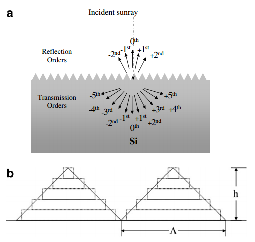
Schematic diagram of: (a) reflection and transmission diffraction orders for incident sunray with pyramid structure and (b) pyramid structure for rigorous couple-wave simulation.
Simulation reflectance spectra of pyramid silicon structures with period of: (a) 800 nm and (b) 350 nm obtained by rigorous couple-wave simulation.
|
|||
Copyright(c) 2008 Nano-optpelectronics Lab., Department of Material Science and Engineering, National Taiwan University No. 1, Sec. 4, Roosevelt Road, Taipei, 10617 Taiwan(R.O.C) Phone:+886-2-3366-3240 Fax:+886-2-2362-7651 |
|||||